

Week 51, 2025
The Semiconductor Newsletter

This edition highlights sustained momentum across the semiconductor value chain, , with SEMI forecasting record equipment spending, Texas Instruments ramping new 300mm capacity, and Rapidus advancing AI-assisted design for advanced nodes. Key developments also include collaborations and market moves involving imec, onsemi and GlobalFoundries, Micron, Qualcomm, and IonQ, alongside KPMG insights on industry confidence and emerging supply chain and infrastructure constraints.
SEMI Projects Semiconductor Equipment Sales to Exceed $150 Billion by 2027
imec and ASRA Align on Automotive Chiplet Architecture Standardization
onsemi and GlobalFoundries Advance 650V GaN Power Technology on 200mm Wafers
UK Consortium Strengthens Semiconductor Metrology for Advanced Materials
Texas Instruments Starts 300mm Production at Sherman Fab, Expanding U.S. Analog Capacity
FAMES Pilot Line Demonstrates 400 °C CMOS Enabling Scalable 3D Sequential Integration
IonQ and QuantumBasel Extend Partnership for Enterprise Quantum Systems in Europe
Qualcomm Completes Alphawave Semi Acquisition to Expand Data Center Capabilities
Rapidus Introduces AI-Assisted Design Toolchain for 2nm Manufacturing Enablement
Micron Reports Record Results as AI Memory Demand Drives HBM Expansion
KPMG Survey Shows High Semiconductor Confidence Amid Rising Structural Constraints
1. SEMI Projects Semiconductor Equipment Sales to Exceed $150 Billion by 2027
AI-Led Investments Drive Sustained Equipment Market Growth
SEMI forecasts global semiconductor manufacturing equipment sales to reach $133 billion in 2025, followed by $145 billion in 2026 and a record $156 billion in 2027. The outlook reflects sustained capital expenditure aligned with artificial intelligence deployment, particularly in leading-edge logic, advanced memory, and advanced packaging technologies. Both front-end and back-end equipment segments are expected to record three consecutive years of expansion. Wafer fab equipment remains the primary growth driver, supported by advanced-node logic investments and accelerated high-bandwidth memory capacity additions. Advanced packaging and test equipment demand continues to rise as heterogeneous integration and tighter performance requirements increase validation complexity.
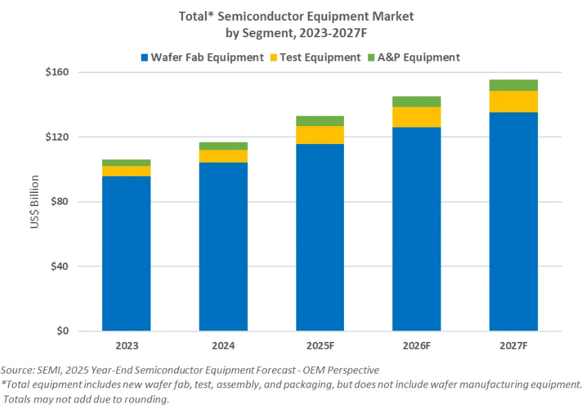
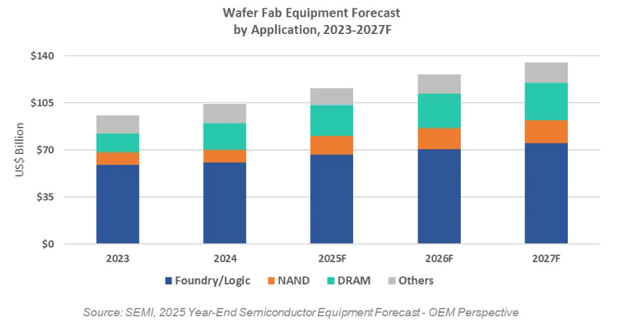
Memory Technology Transitions and Regional Dynamics Shape Demand
Memory-related equipment spending expands through 2027, driven by DRAM node migration and 3D NAND stacking increases linked to AI workloads. NAND equipment sales show strong growth in 2025, followed by steady increases, while DRAM equipment benefits from HBM ramp and yield optimization programs. Back-end equipment growth remains strongest in test systems, reflecting rising validation requirements for AI accelerators and memory devices. China, Taiwan, and Korea remain the largest equipment spending regions. China continues domestic capacity investment, Taiwan sustains leading-edge logic expansion, and Korea reinforces advanced memory manufacturing. Other regions benefit from government incentives, regionalization strategies, and specialty semiconductor investments.
Source: SEMI
2. imec and ASRA Align on Automotive Chiplet Architecture Standardization
Joint Initiative Targets Scalable and Interoperable Automotive Platforms
imec and ASRA launched a strategic alignment initiative to harmonize chiplet architecture specifications for automotive applications. The collaboration focuses on shared reference architectures and interface definitions to support scalable, interoperable system integration. A joint public specification document is planned for release by mid-2026. Chiplet-based architectures address growing automotive requirements for compute scalability, functional partitioning, and extended product lifecycles. Modular integration enables cost optimization and platform reuse, provided ecosystem-level alignment supports multi-vendor interoperability.
Reducing Fragmentation Across the Automotive Semiconductor Ecosystem
The initiative connects imec Automotive Chiplet Program partners with Japanese OEMs and suppliers represented by ASRA. The alignment aims to mitigate risks associated with parallel and uncoordinated standardization efforts by promoting early convergence on architectural principles. Shared specifications support qualification efficiency, supply chain resilience, and long-term reliability targets required in automotive electronic platforms. The collaboration establishes a foundation for broader industry adoption and future standardization activities in automotive chiplet-based system design.
Source: imec
3. onsemi and GlobalFoundries Advance 650V GaN Power Technology on 200mm Wafers
High-Voltage GaN Platform Targets AI and Electrification Markets
onsemi signed a collaboration agreement with GlobalFoundries to develop and manufacture 650V lateral gallium nitride power devices using a 200mm eMode GaN-on-silicon process. The technology roadmap supports power conversion requirements in AI data centers, electric vehicles, renewable energy systems, industrial automation, and aerospace platforms. Customer sampling is planned for the first half of 2026. The collaboration combines foundry-scale GaN process capability with device integration, targeting improved efficiency and power density at system level.
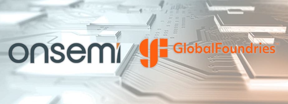
Integrated Power Solutions Enable Advanced Conversion Architectures
The platform integrates GaN devices with silicon drivers, controllers, and thermally enhanced packaging to support higher switching frequencies and reduced system size. Applications include AC-DC power supplies, DC-DC converters, onboard chargers, solar microinverters, energy storage systems, and motor drives. The roadmap expands coverage across low-, medium-, and high-voltage GaN domains, supporting next-generation power architectures aligned with increasing compute density and electrification trends.
Source: onsemi
4. UK Consortium Strengthens Semiconductor Metrology for Advanced Materials
National Program Expands Measurement Capabilities for Compound Semiconductors
RENA Technologies joined a €1.3 million UK government-funded consortium led by National Physical Laboratory to establish advanced metrology capabilities for next-generation semiconductor materials and processes. The initiative addresses measurement and standards gaps associated with compound semiconductors used in power, RF, and optoelectronic applications. The program supports qualification of materials such as gallium nitride, silicon carbide, gallium arsenide, and indium phosphide, which introduce increased complexity in processing and reliability assessment.

Industry-Aligned Metrology Supports Scale-Up and Standardization
Consortium activities include material integrity evaluation, RF performance verification, and device reliability testing under demanding operating conditions. RENA contributes manufacturing-focused expertise in wet processing and surface treatment to align measurement development with fab-level requirements. Priority application domains include power electronics, RF communications, and optoelectronics. The initiative strengthens UK semiconductor infrastructure and supports participation in international standards development for emerging semiconductor technologies.
Source: RENA
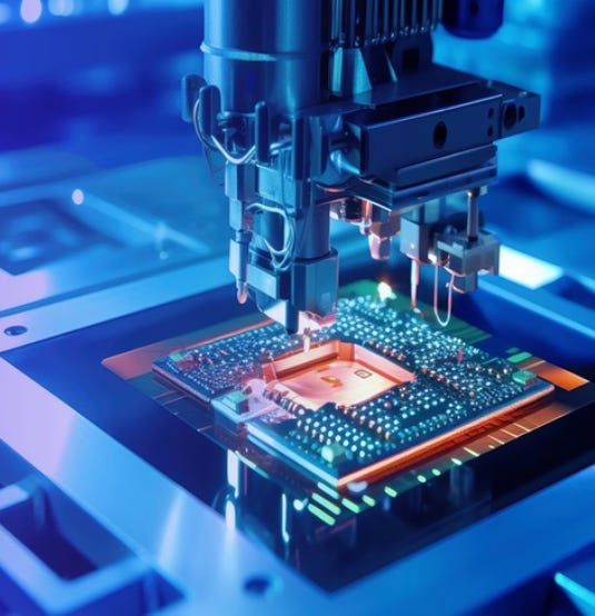
5. Texas Instruments Starts 300mm Production at Sherman Fab, Expanding U.S. Analog Capacity
New 300mm Facility Strengthens Foundational Semiconductor Manufacturing
Texas Instruments began production at its newest 300mm wafer fabrication facility, SM1, in Sherman, Texas, marking a key milestone in its long-term manufacturing expansion strategy. The fab is designed to ramp in line with customer demand and, at full capacity, will produce tens of millions of analog and embedded processing chips per day for automotive, industrial, consumer, and data center applications. The facility represents a continuation of Texas Instruments focus on internal manufacturing control, enabling stable supply, long product lifecycles, and cost efficiency through 300mm scale production.
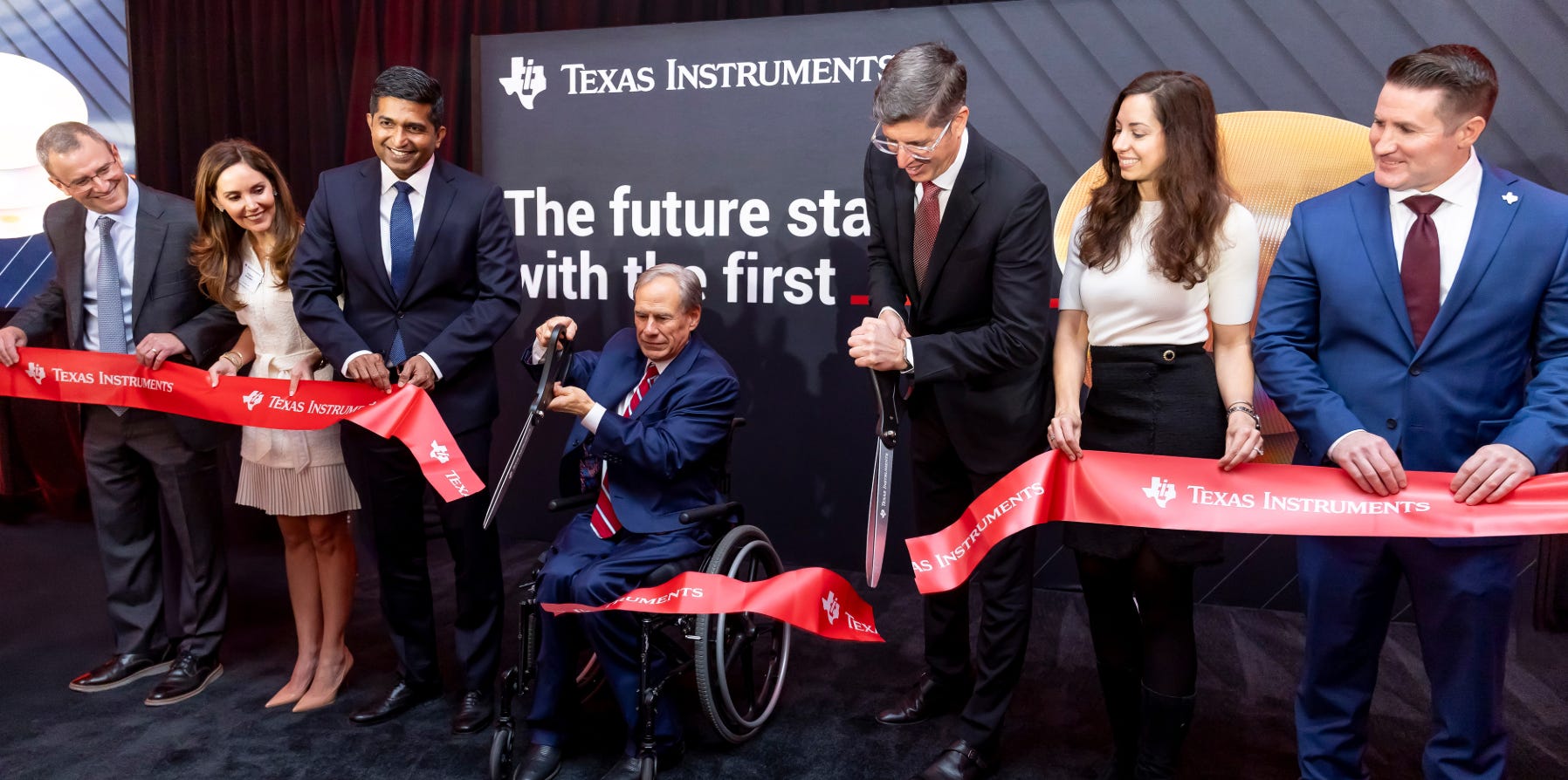
Sherman Mega-Site Anchors Long-Term Capacity Expansion
The Sherman site is planned to host up to four connected wafer fabs, supporting as many as 3,000 direct jobs alongside broader ecosystem employment. The investment forms part of a more than $60 billion capital program across seven fabs in Texas and Utah, representing the largest foundational semiconductor manufacturing investment in U.S. history. By vertically integrating wafer fabrication, process technology, and packaging, Texas Instruments enhances supply chain resilience and positions its analog portfolio to support long-duration customer demand across multiple market cycles.
Source: Texas Instruments
6. FAMES Pilot Line Demonstrates 400 °C CMOS Enabling Scalable 3D Sequential Integration
Low-Temperature SOI CMOS Matches High-Temperature Performance
CEA-Leti achieved a key milestone for 3D sequential integration by fabricating fully functional 2.5 V SOI CMOS devices at a 400 °C thermal budget. Electrical performance matches conventional CMOS devices processed above 1000 °C, removing a critical barrier for stacking logic above back-end-of-line layers. The breakthrough relies on advanced low-temperature process techniques, including nanosecond laser annealing and solid-phase epitaxy regrowth, enabling BEOL-compatible transistor fabrication without degrading underlying circuitry.
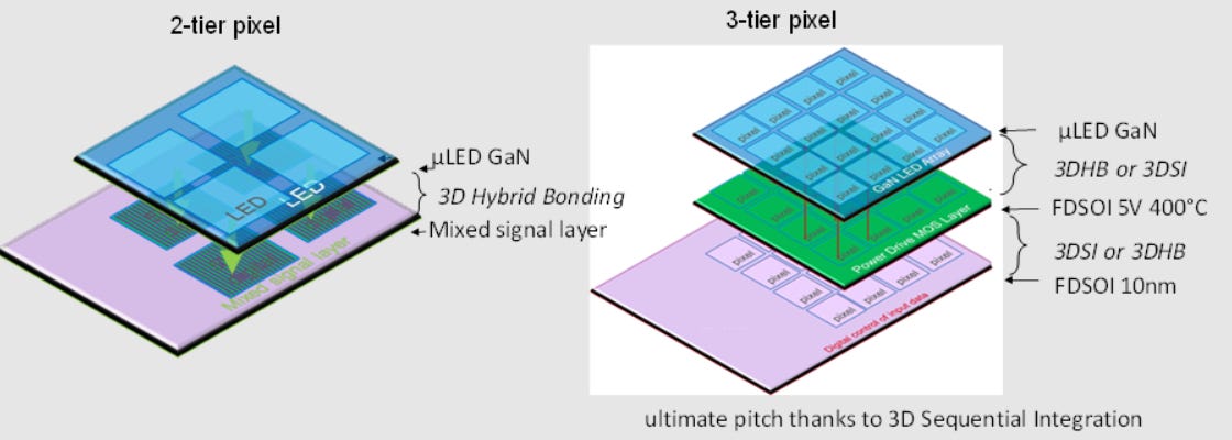
3D Integration Supports More-Than-Moore Architectures
The development supports the objectives of the FAMES Pilot Line, a European initiative aligned with the EU Chips Act. The technology enables dense vertical interconnects and multi-tier stacking that surpasses TSV and hybrid bonding density limits. The approach supports integration of CMOS logic with RF, smart pixel, and embedded memory layers. The pilot line provides an open-access platform for ecosystem partners, accelerating transition from laboratory demonstration to manufacturing-relevant 3D integrated architectures.
Source: Leti-CEA
7. IonQ and QuantumBasel Extend Partnership for Enterprise Quantum Systems in Europe
Expanded Agreement Secures Next-Generation Quantum Hardware
IonQ and QuantumBasel expanded their long-term partnership, extending collaboration through 2029 and increasing total deal value beyond $60 million. The agreement grants QuantumBasel ownership of an existing IonQ Forte Enterprise system and a next-generation IonQ Tempo system. QuantumBasel continues to operate as IonQ Innovation Center in Europe, providing industry, academic, and research access to enterprise-grade trapped-ion quantum computing systems.

Hybrid Quantum-Classical Research Targets Near-Term Applications
The partnership expands joint research programs focused on hybrid quantum-classical workflows, optimization of large language models, and advanced algorithm development. IonQ will also increase on-site technical and research personnel to support system development and collaborative projects. The roadmap includes multiple generations of IonQ systems, targeting higher circuit depth and fidelity to support applications in materials science, logistics, finance, and advanced optimization.
Source: IonQ
8. Qualcomm Completes Alphawave Semi Acquisition to Expand Data Center Capabilities
High-Speed Connectivity IP Enhances AI Compute Platforms
Qualcomm completed the acquisition of Alphawave Semi, accelerating expansion into data center and infrastructure markets. Alphawave Semi brings expertise in high-speed wired connectivity, custom silicon, and chiplet technologies that complement Qualcomm Oryon CPU and Hexagon NPU platforms. The transaction closed ahead of schedule, with Alphawave Semi leadership assuming responsibility for Qualcomm data center business operations.

Integrated Compute and Connectivity Addresses Data Center Scaling
The combined portfolio strengthens system-level optimization for AI workloads, where data movement, latency, and power efficiency represent critical performance constraints. Alphawave Semi connectivity IP supports advanced interconnect standards required for next-generation AI accelerators, networking, and storage platforms. The acquisition positions Qualcomm to deliver integrated AI compute and connectivity solutions across hyperscale data centers and emerging high-performance infrastructure segments.
Source: Qualcomm
9. Rapidus Introduces AI-Assisted Design Toolchain for 2nm Manufacturing Enablement
AI-Driven RTL and PPA Optimization Integrated with Foundry Flows
Rapidus unveiled a new suite of AI-assisted design tools under its Rapidus AI-Agentic Design Solution, supporting the Rapid and Unified Manufacturing Service framework. Initial releases starting in 2026 include Raads Generator, which converts specification inputs into RTL optimized for Rapidus 2nm processes, and Raads Predictor, which accelerates RTL debugging and provides early power, performance, and area estimation for physical design. The tools are designed to integrate with existing EDA environments and will be delivered alongside process design kits and reference flows, enabling tighter coupling between design intent and manufacturing constraints.
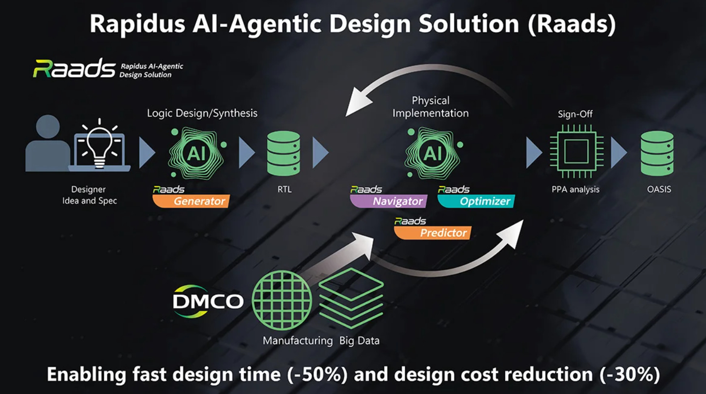
Design Productivity Targets Advanced Node Time-to-Silicon
Additional tools planned for 2026 extend coverage to design quality assurance, hierarchical layout generation, and AI-driven PPA optimization. The roadmap targets reductions of up to 50% in design time and 30% in development cost through AI-supported automation across the design cycle. The toolchain aligns with Rapidus single-wafer manufacturing strategy at the IIM-1 foundry, where automated material handling and 2nm GAA prototyping have entered electrical characterization, supporting rapid design-manufacturing feedback loops.
Source: Rapidus
10. Micron Reports Record Results as AI Memory Demand Drives HBM Expansion
HBM and Data Center Demand Accelerate Financial Performance
Micron Technology reported record fiscal Q1 2026 results, with revenue reaching $13.64 billion and non-GAAP EPS of $4.78, exceeding market expectations. The performance reflects accelerated demand for AI-related memory, particularly high-bandwidth memory, driven by rapid scaling of AI infrastructure. Management projects the total addressable market for HBM to approach $100 billion by 2028, supported by a compound annual growth rate near 40%. Elevated pricing, improved mix, and disciplined execution contributed to gross margin expansion and record free cash flow generation.
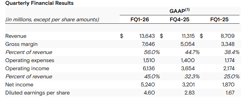
Capacity Investment Supports Sustained AI Memory Growth
Micron increased capital expenditure guidance to $20 billion, aligned with advanced DRAM node transitions and HBM capacity expansion. Fiscal Q2 guidance indicates continued revenue and margin growth, supported by strong order visibility and constrained supply conditions across AI memory segments. The company ended the quarter with $12.0 billion in cash and investments, reinforcing balance sheet strength while funding long-term technology roadmaps in memory and storage solutions for data center and AI platforms.
Source: Micron Technology
11. KPMG Survey Shows High Semiconductor Confidence Amid Rising Structural Constraints
AI Adoption Drives Revenue Outlook Across Market Segments
KPMG and the Global Semiconductor Alliance reported elevated industry confidence, with 93% of executives expecting revenue growth in 2026. The Semiconductor Industry Confidence Index reached 63, one of the highest readings in two decades, reflecting broad AI-driven demand across data centers, memory, wireless communications, and automotive markets. AI leads as the top revenue-driving application, while memory products, including HBM, rank among the highest growth opportunities alongside microprocessors. Companies increasingly deploy AI internally to improve productivity across IT, R&D, and operational functions.
Geopolitics, Energy, and Talent Shape Strategic Priorities
Despite strong demand signals, executives identified tariffs and trade policy as the leading risk, surpassing talent availability for the first time. Energy access emerged as a growing constraint, with concerns over power availability for advanced fabs and hyperscale data centers. Supply chain flexibility and geographic diversification ranked as top strategic priorities for the next three years. The survey highlights a structural challenge: balancing accelerated investment in domestic manufacturing capacity with concerns over long-term agility and innovation under government funding frameworks.
Source: KPMG